I have been threatening to write a blog post on schematics for some time. Schematics are still critically important in Analog and Mixed-signal design. Unfortunately not everyone learns how to draw a schematic in school anymore.
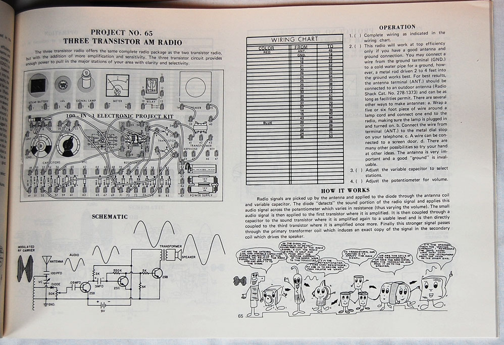
My first introduction to schematics was with my Radio Shack 100-1 Electronics kit. I bought this kit at a garage sale in the 80s. It had three different types of schematics. The three schematics had distinct different purposes.
Old Radio Shack Kit
3 Views (May be too small)
The three schematic views were:
#1. The diagram showing the spring-clip connections required to complete the kit
#2. An Electrical schematic diagram showing the IEEE symbols for the related components.
#3. A "Cartoon" schematic showing how the different circuit elements "helped" each-other to perform the electrical function. In these cartoons transistors danced with LC tank circuits, the speaker was large and loud making sound from electricity.
Ironically it was the "dancing circuits" that I understood last. I don't think the electronics kit was optimally written for a 10 year old learning circuits. I found the #1 and #2 schematics to be most useful given that sometimes there was a mistake in #1. This when I started to memorize schematics in order to help in debug. The above list of schematics reminds me of the "3 Views of circuits".
The three views:
1. Schematic view: Drawn using IEEE or similar symbols
2. Layout view: Drawn using rectangles of different colors (representing different materials)
3. Netlist view: code (text) representing circuits and their related connections.
If you are in analog design you should master all 3 views. This was easier back before Cadence took over the cockpit on Design Automation. In an effort to lower the difficulty of using early CAD software, cadence worked to make everything do-able by a mouse click thereby hiding #3. All views can be used to solve circuit problems, strive to learn them all. More on that in another post..
Back to the schematic:
The Radio Shack schematics were actually pretty good. At the time, I had some magazines from Electronic design magazines such as "Popular Electronics". The old magazine schematics had no real convention and were hard to follow. It turns out that during the "Berkeley Era" analog design renaissance starting in the 1970s schematic methodology improved. Also with good books like Sedra and Smith's Microelectronic circuits we were introduced to a consistent schematic input.
Some key things:
1. Inputs on the left
2. Outputs on the right
3. VDD (Supply) on the top
4. VSS (Ground) on the bottom
5. Clearly labeled currents and node voltages
6. Clearly labeled switches
7. Numerous conventions for ground, signal, earth, vdd, battery
8. Consistent symbols for: Capacitors, resistors, inductors, transformers, tubes, connectors
9. Notes indicating branch currents
10. Notes indicating high voltages
11. Notes to help the layout team understand your design.
12. Good schematic name methodology
13. Logical use of schematic symbols
Far from the "spring clip" days but not too far is the idea that a schematic should convey information. Not a "train-wreck" or "machine generated schematic" but a well drawn schematic can help a person understand, create and even use your circuit.
A good schematic flows with information. Key functions are drawn clearly and near the center of the page. Auxiliary functions are put around the edges of the schematic or at the bottom of the page along with the Revblock. Power-down devices, spare matching devices and the like are placed around the edges often in a box labeled "spare" or "dummies". Input ports are clearly indicated as well as outputs. Avoid drawing in all the NMOS body connections unless you are working on a multi-well process. Drawing clear schematics saves time in that helps the reader understand what the "flow" of the circuit is. Circuits are drawn in such a way as to help the reader. Since we all spend considerable time looking at schematics, its good to spend some time on them. Don't go overboard, since it can be counter-productive. An example is: It is possible to use complicated expressions to connect circuit elements:
node_x<12:4,1,3:2>
I recall (younger) engineers boasting how you can connect up a circuit with a few elements on a page and a list of numbers (as shown above). This is counter-productive for several reasons. For example, during a design review, you will have to explain the connection. You will also have to explain why you chose to hide the connectivity with "cleverness". Your peers will also note that you spent some time figuring out how to make tricky node names when you should have been simply designing a circuit.
Most (but not all) schematics in Analog will be turned into a layout. It is this process of a schematic becoming a layout where most of the trouble in analog comes in. A good designer should be thinking about #1 and #2 above during the design. Yes, you need to visualize the final layout while you are doing the schematic portion of the design. This gets easier with experience. While working on the schematic its important that the layout team be given hints as to what the final form the layout should be in.
Examples of good layout hints:
#1. Identify matching components: M1 matches M2, M3, M4. C1=C2=C3
#2. Identify type of matching: Common centroid, Inter digitized, in the "same row"
a. Also type of environment/area such as "Avoid well edge"
#3. Identify current requirements: Branches identified since 1u copper can only care 1ma of current...
#4. Identify any key pitch required. Some analog layouts are "Row based" and the row geometry should be defined on the schematic
#5. Identify any orientation required. "This resistor match the resistor direction in the Bandgap"
#6. Identify noisy signals that must be shielded against
#7. Identify sensitive signals that must be protected
#8. Identify parts of the circuit that are exposed to light
#9. Identify parts of the circuit that are in the "ESD" network or "Primary or Secondary" ESD structures
10. Identify units for "unit element" type matching arrays
11. Try to avoid components that do not have a layout view since you will be disappointed
12. Bus wires Largest:smallest node<110:0>
13. Bus wires should have thick lines. Single-wires use thin lines
14. Use signal names that are clear and not confusing.
15. Text and drawing layers to help with useful diagrams and notes
Now that we have well annotated clear schematic showing function and giving layout tips, the final task is to give the schematic a good name. Naming conventions on schematics should be such that the schematic's purpose be indicated by its name. Hierarchy is also included in the name. Often the expression "TOP" is used for the top-most level of hierarchy. This is a good starting point. You also would like all the schematics to be "with eachother" and easy to group. Its important that the schematics of a block or subsystem "group" together making them easier to understand. Its counterproductive to keep track of schematics based on peoples names, for example, since they may leave the company or design circuits in several different products. Combining these concepts together I have found that using the circuit name combined with hierarchy work well. With revision control and a title sheet, most all key information can be tracked. In the beginning peoples names may sound like a good way to start but this falls apart after a few products and or process technologies are introduced.
Example of a good set of schematic names:
adc_top
adc_core
adc_analog
adc_digital
adc_refgen
adc_clockgen
adc_stage
adc_stage_comparator
adc_stage_comparator_decoder
If no revision control exists, then you can add further extensions. Often the "rev letter" represents the base-layer generation and "the number" represents the metal connectivity. Normally we prefer to change the metal as this may (sometimes) avoid a "re-qualification" of the product.
adc_top_a1: First metal-rev of ADC_TOP_A0 (a0, a1, a2...)
adc_core_b2: Second metal revision on second set of base-layers (b2)
Never have two schematics of different circuits with the same name. If you want another layout for the same transistor schematic, make a new schematic name with NEW layout comments. Also help the layout designer by letting him or her know that you are leveraging a previous design.
Finally, some schematics are NEVER intended for layout. Those are often "test-bench" schematics or those used for simulation purposes only. I like to name these schematics starting with "zz". I do this since all the test-benches will sit along with eachother in the library when sorted alphabetically.
Finally there are the schematic symbols. If you create your own analog circuits often you will have to provide a "symbol" to allow for the hook-up of your circuit. A good symbol's connection to the rest of a circuit should be obvious. The symbol should have nets clearly indicated and not spaced minimum. The pitch of the symbol should align with the GRID settings used by the team. Its nice to draw a picture on the symbol to help indicate what it does. Often this is a small circuit diagram. Op amp symbols should look like an amplifier. If you have a very large resistor ladder, a schematic can be drawn with a "resistor" on it with tap-points indicated on the symbol. Large resistor and capacitor arrays snaking through schematics can be hard to follow. Sometimes its better if these component arrangements are included within a symbol.
Finally, any special device such as a unit resistor or unit capacitor that is populated in mass on a design should have its own schematic sheet. This is subtle but when a device unit is put on a separate page it forces the layout person also to make an array and not "flatten" the design. This way you can make sure each of your unit elements have the same contact pitch and number, geometry and base-layer connections.
I hope these schematic notes help you and your friends to draw better schematics.
No comments:
Post a Comment