Recently I have been tasked with adding staff to our design team. Like a normal product design team, there is always pressure to get the part done right in zero time. Of course, real analog circuits take time to build, often underestimated by non-experts. Of course most schedule problems come from non-experts making schedules with other experts resigned to pushing back.
So you want to build up your team? Who do you hire? This is a really tough question in reality it depends on what you are doing and what are the key constraints. Is it time to market? Risk? High mask cost? All of the above? Are you adding to a team or creating one from scratch?
In the Radar business the process technology is very advanced and the related costs are high. There also appears to be an unrealistic expectation that first silicon is product worthy. Although real chip designers know this to be unwise, staffing can mitigate the risk of an imperfect chip. The first ingredient is finding someone who has made a mistake and willing to admit it. These characters tend to be older, more mature, have advanced degrees (Ph.D. or MSEE), and have lots of different product experience. The problem with this description is that the older more experienced designers understand unrealistic expectations better than younger engineers. This can help to set expectations. Recently I have phone screened candidates that are afraid of the position I am trying to fill because their perceived interpretation of the risks is too high.
Super senior analog designers often reflect their past. This shouldnt be a surprise, since we are the sum of our experiences. I met one analog designer today who new Verliog, Verilog-A and system Verilog which can be considered "younger engineer" type of skills. Analog was not taught before 2000 with a bent toward system level verification. Chips were small and simple and as the industry has changed more towards system-on-a chip (SOC) these verification tools have increased dramatically in value. However finding an engineer with modern skills who has designs in over 100,000,000 shipped parts/components (for example) is nearly impossible as far as I can tell. This is a message to my mid-career colleagues that its important you pick up these newer verification skills. They are easier to learn than trying to convince a young hard-headed designer to abandon an unreliable circuit or poor layout.
Where is your team? That is also important. Ideally everyone should in the same physical location, but that is no longer realistic. Companies are now keeping track of "High cost centers" such as San Jose where the cost of doing business is high. The value add at these centers needs to justify the high costs. My expectations of engineers in Silicon Valley are high. You should know architecture, circuit design, basic cad and have good communication skills. If you are going to work with remote sites to take advantage of outsourced or "lower cost centers" you need to have good communication skills. I have met some very good technical people recently in my search for staff who have difficult communicating. I don't want to have to have a note-pad to communicate basic concepts.
Team balance is very important. Too many super senior guys can lead to a lower-energy environment. Also not everyone can do the big architectural tasks, so you need a mix of people ideally. I recall discussing this year ago with my friend Perry Heedley using the basketball team analogy. People need to play different cooperative roles working together to get things done. There needs to be trust in the team so I am very sensitive to anyone who may have a reservation about a candidate. This could be technical or personality but there is not any room for a player to bring down the rest of the team. Its not uncommon for me to go through 50 resume's before I get a candidate that fits the team, often with compromises. I am most sensitive to candidates that make me nervous for any reason. I understand people really want a job these days. On Linked-in recently there have been some good short postings in my feed about how to interview. As a hiring manager I read these and a key failing I have seen recently is a candidate trying to "take over" the interview. That doesn't work well with me.
Is the person temporary or full-time? Temporary help (contractors) should be good at communication. Ideally they "get" the idea that they are in themselves a company. The best contractors see themselves as "their own brand" with a service to sell. This includes building the brand reputation including advertising. Some of the best contractors have been high-level managers or people that own their own companies. These guys understand that its not all technical! Problems need to be solved, instructions followed, problems found that are clearly communicated. Not all tasks are have the same cost, the goal is primarily to deliver service. If I can't understand a contractor's English or they are unwilling to come out on-site that is a problem. Also their rate, does it justify what needs to be done? There level of experience? Are they working for a contract house, then why? The absolute best analog engineers I know of all have full-time employment. Recruiters ask me to refer people but the best guys always have a job. Time in-between jobs is also very short in duration, often set by the engineer.
When do you need the person? Good, Cheap, Fast pick two of three. If you need a good person on short notice it will cost a high dollar. If you are willing to put in the time, which is the most realistic approach, you have to staff way in advance of a crisis, otherwise you will sit helpless with a stack of resume's. So planning here and listening to your people's needs are critical.
I am sure a few candidates I have interacted with recently would benefit from this blog. Also there are some good books and references on how to interview. Candidates looking for a job should seek these out, since these interviewing books help the job seeker to understand the position the guy on the other side of the table is. Don't add more work by having a sloppy, long and confusing resume with charts and graphs on your employment history. Don't share too much, make me want to call you! Also, when you do show up, you should have some idea what is expected and what we are doing. This is where the standard preparation helps. What you show up to an interview (empty handed?) will affect my decision to hire you or not. Its important you understand that I am trying to help run a profitable business.
Wednesday, June 11, 2014
Wednesday, March 26, 2014
EE Conference user guide
I like to go to IEEE conferences whenever I can get away which works out to about once a year. My favorite is ISSCC since its in San Francisco and I can BART or drive and some of the worlds best analog designers meet there every year in February. If you are not in IEEE you can still go it just costs a couple hundred dollars more. I have gone 14 out of the last 15 years and realized I have a whole method of getting a lot out of the conference. This blog post is to share some of these observations. Where to stay, how to pick what papers and events, evening panels and finally social hour.
We all are busy as analog designers I doubt many of us work less than 50 hours a week. We are often optimizing what we do. Some of us are more frugal than others it all depends on what is important. To me the important thing is that during the conference "life" is going on and that includes analog. A positive change to your work environment is a nice thing. For adding considerable enjoyment to the event I prefer to stay in the hotel hosting the conference. If my company doesn't want to pay it I will then offer to chip in the difference. If they refuse then I pay out of pocket . Having a room at the event is great since you can setup a remote office there to get things done and keep up back at the plant. I room on a high floor is better since its quieter and the views are better. You normally have to ask at the Marriott for a higher floor. Its easier to get one if you arrive the afternoon or evening before the conference starts after making reservations a couple months in advance.
Day one is when you need to make your schedule final. To leverage the event you may have made a plan with other workmates on what papers sessions to cover. Before the ISSCC this is a first-order plan based on terse descriptions of the papers to be presented. A drawback (or feedback to IEEE) is that its hard to tell if the paper is really interesting or related to what you are looking to learn about at the conference until you get there. The early descriptions are so short that you are forced to show up. Maybe that is the idea anyway. Only after seeing the actual proceedings, now made available online just before the conference, can you really pick what papers to attend. Well you need to check your plan or make your plan by flipping through the papers. Look for easy to read text, clear figures and solid technical content. University papers written by students and their professors are often the best written and easiest to follow. The university papers often don't have the same performance as their commercial counterparts, but the ideas can be easily just as clever. For performance pick the industry papers but you may not get all the detail and there are sometimes empty boxes in diagrams. So I sort through the papers looking for understanding and/or performance and then pick a path through the sessions where the papers are presented. This takes me about an hour to make my plan for the next few days.
Attending the papers is not very easy/relaxing for me. There is a huge amount of information presented. Several years of a persons work (doctoral research) is boiled down to a ~20 minute talk. It takes skill to ramp-up quickly and follow these talks. Sometimes you need to suspend disbelief and re-engage in the end. If you second guess the paper you could miss a few key facts while you ponder. I make a point to write directly on the paper proceedings notes and comments during the papers. I also write down Q/A for papers I particularly like. Q/A can reveal information not in the publication and can also help you learn about other engineers. For example if Dave Robertson of ADI asks about an ADC you need to think about what it was and why. If you wanted to introduce yourself to him for a potential gain in knowledge and opportunity, then you now have a reason. When in school professors scoop knowledge on the students, after graduating it takes effort to keep up and read papers. Working on a network with other engineers is key in maintaining growth and an edge over the other guy.
Yes, analog electronics is one of my favorite hobbies but my love of it is not enough to endure 8 hours of solid technical papers. Maybe a handful of guys out there could attend the entire conference and congratulations. For normal human beings I find it critical to put a break in the day. Normally I schedule a daily nap around 2pm depending on what sessions I go to. I plan my naps on the first day. This is also where the conference hotel really helps out. The nap in the afternoon is critical for me. The talks end as late as 4:30-5pm so a 1 hr nap is not too-long and I bounce back. This is important because after these papers is when things get social when rest is needed.
Ok, I do realize analog guys are not all the most social bunch so we start with a disadvantage. You then combine awkwardness with a wide age spread of attendees, free snacks, wine and beer. Fatigue also is setting in later in the day especially if you didn't have a nap. Part of my writing this post was learning that some engineers are petrified of the social hour. My wife showed me a newsgroup where some people are paralyzed by the idea of going down on the social floor of conferences like these. This is the StreetSmart part of the post, how to do the social hour. Some of the social tips follow.
Advances in technology (text messaging) are not doing well with the age gap issue at ISSCC. Some of the most experienced and distinguished engineers may not use text messages since the go through most all of their lives without it. The younger the engineer the more tech savvy. Its my observation that the youngest engineers rarely interact with the most experienced senior designers. Also, some of the other-way around exists, some older engineers avoid the younger and its sad. When approaching a professor or famous circuit designer you need to approach them in a way that is most comfortable. Don't interrupt but wait to be invited into a conversation. If you want to talk to someone its better if they are finishing up talking to someone else or not talking to someone you do not know. Make eye contact that is normally enough to let someone know you are interested chatting. Also asking if they have time is nice, since if they are busy they will appreciate it. When you see them next there is a much higher chance they will engage. Be aware of people around you who may also want to talk to the same person, be polite and watch body language. If their feet or body turn away its time to wrap it up. Its important you have a reason to talk. The easiest conversation starter is to ask about a paper presented earlier in the day or made during paper Q/A. Poster session reactions work too. Ask what they thought of it. Alternatively you can ask about a paper, presentation or book written by the designer. Author interviews are also a great place to meet people and will give you a connection.
Whatever you do DO NOT drink too much at social hour. Sipping one glass of wine or having a beer is fine but more than two and there is trouble. You are interacting with some really intelligent people and its a rare opportunity. The impression goes both ways, if you drunkenly stumble into someone you are not going to make a friend. This is a common mistake since the free-beer thing takes a little will power for frugal engineers. Some engineers wrap a paper bar napkin around the beer and carry it around. I know of at least one famous professor who does that too. The bar napkin is good since it helps you to NOT peel the label making it less obvious that you are "carrying the beer around". Tired and tipsy is not a good combination for making it easy to meet new people. If you are part of the text-message generation or new to the United States then I suggest you observe before engaging. Most engineers are there to have a good time so project positive energy and things should go well. At the social hour I normally make dinner connections. After the social hour is the time to have a few drinks and talk about circuits.
The evening panel sessions occur after dinner. These vary in content some being more serious than others. The best are the debugging/analog guru sessions with the colorful characters of the analog integrated circuit community. Young and old I often wonder what it takes to get on one of those panels it seems like a strong network helps. Panel arguments about tubes vs. transistors or BJTs vs. FETS can get spicy and absolutely hilarious. The analog community respects and laughs at itself in these sessions.
After the conference is the best time to write down any final notes. Life is busy and its easy to forget the details or interesting techniques learned during the conference. Not all from the papers, some from fellow engineers. Take inventory of business cards, you can write notes on the back about the people. This information helps later the following year since you can build on the history. People like to hear about themselves, its all good.
Going to a conference can be an expensive and take a chunk of time. If you plan your time well you can make the conference a fun, educational and rewarding experience. Be careful to pace yourself since the material can overload even the most experienced engineers. Use the social hour to connect, challenge yourself to meet someone new and don't drink too much at the social. The IEEE has been continuously improving the conferences over the years, so if you have not been to one in a while it may be time.
Monday, January 20, 2014
Uneasy Pease
From my bad interview at a no longer existing analog company along in 1993 along with a downturn in the economy I decided to focus my education in the California central valley and everything related to it. (..."Please wait for the CEO he will see you next", that was after a long afternoon of technical interviews without even a snack break, with low blood sugar, I responded "Don't bother", took off my badge and walked out the door and back into graduate school) I had my electronics hobby kits, the recording studio work, automated laundry repair etc to deal with so I wasn't into Bob Pease and the analog scene being (heavily influenced) by National Semiconductor in the early 1990s. I noticed in my visits to National that they had excellent analog designers and I will mention a few. Its been flattering to hear feedback that my posts remind them of Bob's writings so I thought its time to "dig up" Bob.
This posting is basically an old school book review of Bob's Kindle book on Troubleshooting analog circuits. With practice my writing should get better and become more like Bob's. But first more about Mr. Pease.
I recall a SSCRL (UCD Seminar) where we had a guest speaker Bob Pease (1994?). A somewhat frail looking graying and bearded man with numerous cutout foils for the overhead projector. His presentation was about a front-end of some kind I recall he was interactive and asked questions to the group as he went along. In a mechanical fashion he would uncover paper to reveal new information in the overhead transparency. (In the old days we had these projectors with this clear film...it was analog...) His talk was pretty good, low-tech and down to earth entertaining. Bob was an expert interacting with other engineers and there were more than a few laughs while he disarmed difficult to gather analog concepts. His talk was second best unfortunately that year beat out by Rich Reay who gave out a six-pack for nailing the old common-emitter gain problem.
My next interaction with Bob was when I visited National Semiconductor as a scholarship award winner. Bob wanted to meet us it was important to everyone including Bob. Funny I remember the museum they had in the building with old electronics that was really cool. Glass cases with old shiny analog guys like me like that stuff. The door gift for the awards was an analog clock. I recall the clocks all lined up with their hands in different random times at the beginning of the event. Then the clocks were passed around to me and the other award winners. As we left on a tour a looked back in the room and all the clocks were correctly set.... engineers and OCD. Then a couple years afterward there was my interview at NSC in 1998 where my visit to Bob required me to brave his "dual cubicle" and find him in the corner between stacks of papers. He shook my hand, promptly reached into a corner and pulled out a poster of "Bob Pease Lord of the Bandgap" which he promptly signed and sent me on my way. My friendly host Pat Tucci and the creative Sing Chin made for a good day of data converters and at least one display chip. My Bob Pease poster was donated to the Lab and I don't think it was unique.
Now some 16 years later I had a credit on Amazon so I purchased a rather expensive Kindle book "Troubleshooting Analog Circuits" by Robert A. Pease ISBN 0-7506-9949-8 c 1991 for $37.54 soft-copy. You would think this would be an enjoyable read for many but this was my first exposure to Bob's writing and how his mind works. His writing and reasoning are amazingly clear following a logical progression. He comes to good conclusions with his solid understanding of the underlying physics of electronic devices. When it comes down to it we electrical engineers just apply physics to make money for our employers. Bob's book can be summarized as observe, be aware and think. Seek out the physics as to "why".
The book is quite excellent including photos and clearly drawn schematics. Some books don't look as clear in their Kindle form but this is an excellent conversion including the figures. In the first chapter he covers cost oriented test equipment. Good advice of course about getting the most accuracy out of meters. Choose the right tool for the job its basic to Bob he was trying to do the best at bench analog. His test instruments are cheap and aimed more at low-frequency DC/DC converters and the like, its important to understand what Bob was working to get the most out of it. It also helps if you have seen some of these old components before, you should know a 2N3055 in a TO-3 will leave a welt if it hit you on the head. A TO-220 has a screw tab on it, so on.
Bob covers passives in chapters 3 and 4 including noisy resistors, film, wire-wound with their smokey charred failure mechanisms. (He didnt mention you can identify the bad component by the smell, so basically many analog gear-heads know what different parts smell like when they burn such as the fishy burnt aluminum electrolytic.) The inductor section actually hurt to read. Yes the saturation current of an inductor decreases at temperature. No, the inductor is not the same after you hammer it with current, that took me and a team of guys at least a week to figure that one out. Bob could have saved me a weeks there and at least of lab pain. (abused inductors can de-solder themselves) Dried capacitors (seen that) bad electrolytics without bias, oil filled, anything with "ene" is high performance and tantalum caps suck for Q. Type of capacitor dielectric hurt too (I know guys who have spent weeks debugging poor choice of dielectric in a DSL application) they could have benefit from these two chapters. I think I could have saved a few gray hairs and months of debug over the years had I got this book earlier. Bobs chapters here remind me of Henry Ott's book on Noise Reduction Techniques in Electronic Systems (1988 John Wiley ISBN 0-471-85068-3).
His section on board issues has a bit of the self inflicted in it. Bob lived on the board, 3-d circuit design-fly wire. Air is an excellent dielectric seems more of an excuse to stay with what works. This is the way he understood things. He wasn't into the SSA "the three views" (covered in a an earlier post) wherein the text-netlist can be hacked like his 3-D circuits. Hacking the input simulator input netlist (ASCII) is akin to his 3D lab experiments but in a sterile environment. This power would scare Bob for sure with his dislike of computers, however if he were to have leveraged his approach on the simulator who knows where we would be. (No I am not saying bench work is obsolete.) I my work I try to avoid situations where the physics is so sensitive that a single fingerprint or a misting of flux can wipe out the performance. Physics will dictate exactly what your circuit does, always. From a street-smart standpoint it sounds to me like it may be a good idea to integrate sensitive electronics since the package will protect the internal high-impedance nodes. Put thermally sensitive stuff close together. What matters to the customer most is the solution in the end. Having circuit boards so sensitive makes me wonder about how robust board will be in the long run especially when you don't know what the customer is going to do with it. I think of random environments such as a guy who travels frequently with the equipment to a smoggy desert, then a dry polar cap all along blowing cigar smoke at the installed board. Of course Bob would just put the board in the dishwasher that should clean off the smoke.
He covers wearing out Zener diodes, how Zeners actually avalanch over 3V, ok following been there but key to understand. (Michael Altmann taught me a few things about Zeners he may have learned from Bob before going back to Intel.) Bob next talks about finger debugging, the capacitance of a finger loading a circuit, yes fingers are useful in debugging and I have had my share of shocks and burns, still Bob keeps going down the practical debug path. Even with a stocked lab Bob would use everything in his arsenal to debug. The fuse section is excellent I think many of us don't know AC vs DC and fuse ratings this was good. We have all seen transistors sacrifice themselves to protect a valuable fuse, not much on that in the book though but it seems like something Bob would write about. Resistive diodes, blown bipolars and MOS we have all have seen our share of those. The leaky 1N914 section was excellent while not a big surprise to hear about since I preferred the germanium diodes in crystal radios since the gave more volume than the 1N914. Bob is an expert at DC DC converters (ironically my least-favorite circuits) having fixed numerous bad boards stuffed with non typical components required for typical designs. He reminds me again and again of how I don't like those circuits (because often their failure can be catastrophic). Its hard to debug a chip when you pour its innards out of the package into a heap of glass after a fail. (no, it didn't melt-down when I was done with that circuit but the horror) Some DC DC converter issues are audible but that part of my hearing was blown out long ago by stress testing audio power amplifiers with Led Zepplin, The Who and sonic holography experiments involving reproducing actual recordings of freight trains (the Mach 5 experiments~1990). Bob doesn't mention audibles his hearing was worse than mine.
So in general if you have not read Bob's book I highly recommend it. This is especially true for "non-hobby" types or people who have picked up their analog later in life. The years have changed analog and those old exposed connections are now buried inside some little device or surface mount pc board. We in the industry have been working hard to make sure new hobby guys find analog as intimidating as possible with microscopic difficult to deal with components. If this is your first exposure to practical electronics is the university you should rush to by Bob's book, although it does show some age. One thing to consider is that the knowledge in the book is decades of experience so the $37 for a Kindle but is a steal! (I sadly estimate Bob's book could have saved me 100s of hours. Some hours, in a crunch time for example, you can never get back!)
Reading Bob's book made me wonder how relevant it will be another 10 years from now. Its doing very well by the way as the entire industry is changing. (Physics doesn't change fortunately). We are trying to get the human out of the system as much as possible since we are imperfect, make cold solder joints occasionally and miss a color code multiplier. Bob's techniques of circuit analysis and phase margin checking are useful but few people now build up something without simulating it first. Do not let that the simulator think for you but help you think. You can still ponder what is going on and why the result may or may not be accurate. In fact its critical you do so. Do I believe the result? That is a key reason why we go to school and learn physics and engineering. Those people who work along side me know I distrust new tools and flow without independent verification. I hate tool and software changes. Bob had it correct that simulators can impair circuit thinking if abused. Simulations are garbage without thought. If anyone from Cadence is reading this please allow us to purchase a release with only bugfixes and NO new features to break and or screw up other working features. We are not allowed to re-compile our multi-million dollar masks its hardware.
Personally I am a big fan of the simulator since when driven by an expert it can enhance understanding. We take it for granted that we can look at any signal in the simulator and get a waveform representing what is happening at that spot with respect to time. After working on a circuit the designer gets an expectation of what to see at various points. After a while, this gets committed to memory and we can be "surprised" when we don't see an expected result we understand. After years of staring at simulator outputs and anticipating results I can now see waveforms in my mind. (My internal transient simulator I call it I am not unique in this ability since many of us have it). I can debug circuit problems anywhere even while driving or on a cross country flight. Often I have a parameter sheet from the process so I can do hand calculations. For me as a simulator all I need is rest, a good meal and time to focus. The biggest challenge is the latter.
Using Bob's analog "3D cloud of circuits" approach on the bench is akin to an expert hacking on a netlist input to an analog simulator. At this point in my career I can visualize a smaller circuit in my mind and write an HSPICE deck off the cuff to simulate it. There is an added advantage here with a simulator since the elements are ideal, don't require soldering and infinite component values are available. This sounds harder than what Bob due to the open ended flexibility but it all depends on your perspective. I am not alone in this ability visualize circuit netlists as circuis and most good people I know debug or track down issues in an any of the three views. In simulators tolerances can be checked in sim cases, voltage sources are perfect as are current sources, volt-meters have no load at all. If desired, devices can be matched perfectly. All connections are perfect in a simulator making soldering skill a moot point. You can quickly and perfectly connect any two or more nets with a few lines in a SPICE deck.
In an enlightening section in the second half of his book Bob demonstrates how difficult a reliable test-board can be to produce. I take this as a challenge as an engineer to make the final product as insensitive as possible to external elements (within reason). Bob has some good points but if you can pull sensitive components inside the chip there is much to be gained in terms of resistance to handling. If the passive device is not present it can't mess up or go bad.
The scale of electronics is changing. The discrete components are expensive for our customers and take up valuable board space. Complicated circuits (such as a calibrated ADC) cannot be hacked together on the bench easily. The simulator has its purpose. Bob's book is still useful today because the physics of the analog situation has not changed. As long as the physics remains so will Bob's book. Buy it, Read it, Live it!
-----------------------------------------------------------------------
SSA Announcements:
Saturday 1/25/2014 San Francisco Yacht Club
UC Davis Engineering Awards on January 25th in San Francisco where Stephen will accept his teaching award.
February 2/9/2014 through 2/12/2014 ISSCC 2014 San Francisco
I will be attending the ISSCC 2014 in San Francisco from 2/9 through 2/12. I will be staying at the hotel.
-Ken
Tuesday, November 19, 2013
Analog RESETN
RESETN = !RESET or "not RESET" no.. thats not a typo. Analog guys be careful!!
Reset.. how bad could it be?
A common theme for mixed-signal conversations has to do with the chip RESET function. We all take for granted that when we turn on electronics they always behave the same way. It turns out that many designers spend time behind the seems to insure a consistent experience with their chip.
The way to make a chip behave each time is to have a RESET circuit. A IC's RESET function normally is comprised of several different circuit blocks. These blocks work together to insure that the chip always starts from the same initial state. Some chips have firmware or microcontrollers so they can remember a previous state. This is not what is being discussed here. Before that microcontroller "wakes up" to put the device in a known state, is has to come up in a known safe state to begin with. That is what the RESET is for.
The first part of a RESET system is an element that creates a reset event. This event could be a pin on the chip that needs to be temporarily set to 0V. Other methods look for a rising edge on a power supply, others look for the power-supply to get above a certain level. Hysteresis is important since clearing the RESET state often involves a dramatic increase in current consumption. Without hysteresis the inrush of current can cause a mini brown-out and can even cause oscillations as the circuit comes in and out its reset state. Even more complicated RESET systems look for the presence of a clock (clock detect), holding the device in a safe state until the on-chip clock generator and possibly multiple power supplies come online. In practical implementations I have seen several techniques used in practice. People have their favorites but often this is shaped by the products they design. The toughest resets I have worked with have been those required for cell-phones (the battery removal problem).
The reset generation circuits are a class that must operate with very low supply voltage. The skilled designer needs to make sure the power-on circuit behaves on power up and discharges (how the reset circuit resets itself) on power-off. There are common circuits but in practice some of the hardest to build. The reason being is the design space includes a supply voltage of 0. It is common for circuits like these to include resistors since they still can pull a current when there is not enough voltage to turn on a transistor. Capacitors can also be used to siphon current from the supply ramp, its normally washed out by an external bypass cap the inrush added by this is trick is small. These circuits should be Monte-Carlo'd and have the ability (ideally) to be disabled via an external pad/pin, bond-option, fuse or FIB target on the layout in a high metal layer. I'll do another blog post on RESET disasters. If your reset circuit has more than 30 or so devices you are doing it wrong! Simple is better!
The second important key part of an IC reset subsystem are the circuits that receive the master RESET signal from the above listed set of reset detection circuits or pin. These circuits distribute the RESET and implement the clearing of the memory/previous state. There are two classes of RESET that are employed, asynchronous and synchronous reset. The asynchronous RESET works without the presence of a clock. Normally this is distributed as RESETN (!RESET) and is held high until the chip is allowed to run (low). These can be connected to a resistor and capacitor off-chip and often (but not always) come out of the chip as a pin. The synchronous reset happens on a clock edge, allowing (in theory) several chip systems to come online at the same time or in a known (reliable) sequence. What I didn't learn in school was how tough making a product quality RESET can be.
I will guess most of the people who read this blog have struggled with a RESET issue at least once. Its normally a test setup killer since you can lose control of the state of the chip. Customers get unpredictable results. Chips randomly burn up. Experiments may become non-repeatable since some internal circuits could be affected by a previous experiment. Work-arounds include driving the reset pin off-chip and using a serial port to force every state before the chip is used. The old "hidden state" problem is a big pain.
The good news is that there are experts in RESET. This is where our digital designer friends can make a huge difference. I know analog guys think they are smart but its Street Smart to leverage digital design experts on how the reset works at nearly every level. A good whiteboard discussion. Digital designers are also good at making sure (by design) that their digital circuit does reset properly. I know at least one other guy who has written a script to check a digital design (from analog person shhhh) for flip-flops without a reset (and found them!). A flip-flop is not just a flip-flop. Think about it before putting on the schematic. What happens if its not reset? Sometimes its ok and other times its not.
The digital verification tools can check the reset function for hidden issues such a sequencing with proper modeling. The digital designer can't even launch a simulation run until the basic initial (RESET) state is set. Also some resets must take longer than others or may depend on other things happening in the chip. An example of this is power-gating where parts of a chip are shut down to save battery life. When the power islands go up and down the digital needs to act predictably. The new power island techniques add yet another level of complication.
When it comes down to it, the start-up state and how to get out of it should be a priority early on in your design program. Make sure you have (ideally) proven reset IP and thank the designer who provided it. If you need to design your RESET circuit, make sure a gray-beard with related experience is available. Finally the RESET sub-system should be designed, simulated and verified by a qualified event-based style (DIGITAL) design expert. Reset is not something you simply "psych out" unless your chip is supposed to smoke.
Wednesday, October 30, 2013
So you have to design something new?
I am now reaching a bit for posts but this one comes to mind every now and then. Its basically a process you can go through to create a new circuit.
So it comes down to it your name is drawn from a hat or your manager comes by and says "we have a problem we need you to solve...". What do you do?
Creative problem solving requires thinking. Not simply voting on the best idea or gathering around a fire and singing songs. As engineers we are paid to think. I am frustrated lately by colleagues who want me to convert my experience into a simple methodology or simple procedure eliminating a thought process. "Thinking hurts" - For me at least, I do feel some mental discomfort when solving a tough problem, this feeling is temporary and is feedback in some ways that I may not be taking the best approach. Of course it all depends on the problem and the situation. In general the problem solving method described here is the same, however the constraints are different for each problem. The goal should be described as accurately as possible an understood before starting.
What is it I need to build??
Well, the first part of problem solving is understanding the problem. Some less experienced analog managers always think that the designers are "pushing-back" or asking for justification of the design. (I may have heard that on the phone today even.) This is almost always misinterpreted as an attack, but an analog designer understands how much effort will go into the work. I never take design casually even if its a basic one. The first step is always getting more information on the problem that needs to be solved. In some cases, a circuit design is not even required. There could be a feature or a way of configuring another circuit to eliminate the need for a new one. Getting information including maximum power consumption? When the circuit is required? What modes require it? how big can it be? whats nearby on chip? Does it touch a pad or signal that goes off chip? Does its non-function render the chip useless? Does it have any special requirements such as 10,000V ESD or high DC voltage? Does it interact with circuits off chip? Does it operate at 60GHz?
Is it all unique?
Is the design completely new in a new process or is there an existing design that can be leveraged? Getting a good analog circuit in your process technology can be a huge leap in getting the circuit done on a short time schedule. Some people do not like to use other people's circuits (called NIH), however those are normally designers that have taken more than some abuse. Even getting schematics and simulation test-benches from another designer can same time. I try to avoid starting with a blank sheet as much as possible. So first thing after understanding is an "IP" search. Now something behind the times is the ability to search for IP within a company. I worked on a idea with a friend (Anasym) on an early concept of this technology. The next best thing is a good memory. I have discovered that in the San Jose area, many of the better analog circuit designers are capable of memorizing many of their own as well as their colleague's circuits. "I think I saw a similar circuit on the LXT9785, Sumant designed it, ask him." Also your network inside the company helps, talking to your manager or an engineering director/vp and they may have an idea. Normally its good to ask around at the beginning since people can give their inputs. Finally when you get to the design review it will make sense to them, and if you used one of their ideas your design review should be all the smoother. Another place to look for circuits is in the literature such as in textbooks and/or the IEEE Explore. I pay $35/mo for IEEE explore and its well worth it. I have pulled several circuits out of there, stick with bigger university names and avoid the small conferences.
Break it into bits:
Any circuit of significant complexity has more than one device. Normally there are groups of devices that need to work together to complete some sort of function. For example, 5 transistors may be grouped together to form an amplifier. This amplifier could be part of something else. So after getting information and previous circuits, the next step is to partition the function. Normally this starts as a block diagram or sketch. Often some hand calculations are required, what is the jitter? How much noise can I handle? Is a decoder needed? Memory? How will I test it? All these and more constraints will help define the architecture of the overall circuit. I always try to go for simplicity first, then increase complexity as performance requires. If you can get away with one transistor and meet all specs, more power too ya. The more elements the more iteration is needed since there are almost always trade-offs. I like breaking designs into pieces if possible since you can leverage parallel resources (people) to assemble your design. C, Matlab, Simulink, System Verilog, Verilog-a are all ways of refining the architecture by means of behavioral simulation. Hand calculations, math and behavioral simulation help to determine the specifications of the sub blocks. Normally I write a "master document" covering the top-level of the proposed design as well as some architectural comments on the sub-blocks and how the specs were determined. If you are lucky you may have a system team or applications team capable of helping with the performance requirements. Once you have broken the block into partitions, then its time to start.
Where do I start?
Well at this point you have a analog "system" of some sort with circuit ideas and blocks but you don't know where to start. One method I find to be very useful from Covey is "Begin with the end in mind." That is, start designing the circuit at the output. I find this useful for DACs, transmitters, voltage references and buffer amplifiers. Often the load and its electrical properties define the circuit driving them. Find the largest and most difficult subsystems and then size them up next, if they are not already at the output. Large blocks are expensive chip wise and should have thought put into them up-front. This is especially true if the circuit is repeated many times. Also, "op-amps are always way bigger in the layout than expected." So be careful trading re-use of area intensive or non-optimal circuit blocks when high repetition is needed. The next thing I would look for after big blocks are blocks with high impedance. Those blocks are very low-power circuits and very high-gain amplifiers. These circuits tend to be very sensitive to their environment and may actually require interaction with the environment. For example, if you want a constant voltage somewhere you probably need a bias current that tracks your resistor sheet resistance. Others circuits exist (Constant-gm, proportional to temperature, voltage.. etc) that track out elements in the environment.
Review it:
Your peers are your best bet at finding the best solution and or smoking out a bad one. (Not every idea I have is a good one. Its ok to admit that, its street smart.) This requires exposure to other peoples opinions, who should understand that you are "out there/exposed" when doing a design review. I don't think anyone really likes doing a design review, but they can be insightful. Maybe the circuit already exists and you don't know about it? Possibly a circuit can be copied from another chip or ported to the process of the present chip. Maybe the problem was "over thought", having additional complexity which requires more complexity to manage. (band-aids when they are not needed). Ideally you should send your design review material out ahead of time for the team to review. Some people don't absorb information or bring them selves to communicate as quick as others so this allows everyone to participate.
Don't be afraid to get experts involved or leverage from them. Reading the recent IEEE article on a noted brilliant but tough analog designer I didn't agree that a design review has to be a painful experience. I understand the more experienced trying to make an impression, but there are more powerful approaches that motivate through understanding. The analog industry is changing, the age of the "crazy analog guy" is over. You need to make an effort to connect with your company's experts, since they are often busy/overloaded. However, a good expert should help a less experienced designer since it will improve execution and the success of the company.
Cost of the circuits:
The cost of your circuit is in design time, performance and area. The goal is to try to find the balance custom tailored to the circuit problem at hand. The first priority should be functionality followed optimization. In some cases there may only be one solution, and in others many.
To make things more confusing, the correct answer is also process technology dependent. In an older process such as 0.35u digital logic gates are expensive and fewer routing layers are available. Analog solutions can do wonders with the higher available power supply in that process. However, in deep submicron (ex: 32nm) analog solutions can be expensive compared to one leveraging digital. Lower supply voltages in deep submicron combined with device noise. Deep submicron does have its advantages with matching. Since the devices are closer in proximity, the process control is better and analog components such as capacitors match better. Devices also match (locally better) than in the older processes especially when using large device sizes. Klaas Bult wrote about the benefits of scaling in "The Effect of Technology Scaling on Power Dissipation in Analog Circuits" Springer 2006 in his conclusion.
"Matching dominated designs exhibit a decreasing or equal power dissipation for shrinking technologies whereas noise dominated designs show an increasing or equal power dissipation. " -Klass Bult
Noise dominated designs are those with many active devices operating with large bandwidths. An example of a "matching" dominated design is a flash or SAR ADC. A pipelined/algorithmic ADC would be considered noise dominated by Klass.
How long..?
Finally there is the design time involved. Over the years I have related this to analog device count. The more analog circuitry the longer the schedule. When in doubt, I do a devices/per_day evaulation and multiply by a factor depending on the performance of the block based on my experience. Combined with a difficult (or worlds best) performance spec this can eat up considerable schedule. Marketing often has demands to have many features/modes/functions for an analog design. These sound great but can lead to huge verification times. Also, spec changes late in the game often require re-work of other blocks. Sometimes, the late additions can make a design impossible to complete in the time and area available. The later the change, the higher the cost which increases exponentially on complex designs. This is a huge problem in the industry since re-work and cancelled programs lead to poorer work quality and more of the same. The reason for the complexity creep is that the larger designs have more interaction between the blocks. As Mr. Scott from Star Trek said "The more plumbing the easier it is to stop up the sink". Since so few people have worked on larger designs the cost of verification of a new function can be shockingly high. In addition, if a picky customer forces extra verification or their own methodology this should be accounted for in the schedule. Its easy to say "layout extracted monte-carlo 500 times over 26 process corners please". However mixed signal simulation extracted 500 monte-carlos that may not be possible to to take months using a 100 CPUs. PLLs are notoriously tough due to time constants and harmonic balance simulators don't find everything. (I recall a 2^-22 bit error rate transient sim monte-carlo ADC request some years ago.) You could send the chip to fab and get the results faster. In fact, if that is the case do it since its more accurate! Again.. paid to think not just turn a crank. This is not implying that you shouldn't check for or understand what random effects occur inside your circuit. Monte Carlo is also good as a tool when an analog designer wants to focus on mismatch in a part or section of a circuit. This needs to be judged depending on cost and schedule.
In summary, break complicated design problems into manageable chunks. Think about what you are building and what you want in the end up front. Leverage existing knowledge of your peers, IEEE publications and books. Try to "wing it" as little as possible since innovation can sometimes have hidden pitfalls, so innovation should be focused. Your ideas (architecture) should be run by your peers before you pour a lot of effort into solving the circuit problem at hand.
Next up... RESET
Monday, July 1, 2013
Schematics - passed up by progress?
I have been threatening to write a blog post on schematics for some time. Schematics are still critically important in Analog and Mixed-signal design. Unfortunately not everyone learns how to draw a schematic in school anymore.
My first introduction to schematics was with my Radio Shack 100-1 Electronics kit. I bought this kit at a garage sale in the 80s. It had three different types of schematics. The three schematics had distinct different purposes.
Old Radio Shack Kit
3 Views (May be too small)
The three schematic views were:
#1. The diagram showing the spring-clip connections required to complete the kit
#2. An Electrical schematic diagram showing the IEEE symbols for the related components.
#3. A "Cartoon" schematic showing how the different circuit elements "helped" each-other to perform the electrical function. In these cartoons transistors danced with LC tank circuits, the speaker was large and loud making sound from electricity.
Ironically it was the "dancing circuits" that I understood last. I don't think the electronics kit was optimally written for a 10 year old learning circuits. I found the #1 and #2 schematics to be most useful given that sometimes there was a mistake in #1. This when I started to memorize schematics in order to help in debug. The above list of schematics reminds me of the "3 Views of circuits".
The three views:
1. Schematic view: Drawn using IEEE or similar symbols
2. Layout view: Drawn using rectangles of different colors (representing different materials)
3. Netlist view: code (text) representing circuits and their related connections.
If you are in analog design you should master all 3 views. This was easier back before Cadence took over the cockpit on Design Automation. In an effort to lower the difficulty of using early CAD software, cadence worked to make everything do-able by a mouse click thereby hiding #3. All views can be used to solve circuit problems, strive to learn them all. More on that in another post..
Back to the schematic:
The Radio Shack schematics were actually pretty good. At the time, I had some magazines from Electronic design magazines such as "Popular Electronics". The old magazine schematics had no real convention and were hard to follow. It turns out that during the "Berkeley Era" analog design renaissance starting in the 1970s schematic methodology improved. Also with good books like Sedra and Smith's Microelectronic circuits we were introduced to a consistent schematic input.
Some key things:
1. Inputs on the left
2. Outputs on the right
3. VDD (Supply) on the top
4. VSS (Ground) on the bottom
5. Clearly labeled currents and node voltages
6. Clearly labeled switches
7. Numerous conventions for ground, signal, earth, vdd, battery
8. Consistent symbols for: Capacitors, resistors, inductors, transformers, tubes, connectors
9. Notes indicating branch currents
10. Notes indicating high voltages
11. Notes to help the layout team understand your design.
12. Good schematic name methodology
13. Logical use of schematic symbols
Far from the "spring clip" days but not too far is the idea that a schematic should convey information. Not a "train-wreck" or "machine generated schematic" but a well drawn schematic can help a person understand, create and even use your circuit.
A good schematic flows with information. Key functions are drawn clearly and near the center of the page. Auxiliary functions are put around the edges of the schematic or at the bottom of the page along with the Revblock. Power-down devices, spare matching devices and the like are placed around the edges often in a box labeled "spare" or "dummies". Input ports are clearly indicated as well as outputs. Avoid drawing in all the NMOS body connections unless you are working on a multi-well process. Drawing clear schematics saves time in that helps the reader understand what the "flow" of the circuit is. Circuits are drawn in such a way as to help the reader. Since we all spend considerable time looking at schematics, its good to spend some time on them. Don't go overboard, since it can be counter-productive. An example is: It is possible to use complicated expressions to connect circuit elements:
node_x<12:4,1,3:2>
I recall (younger) engineers boasting how you can connect up a circuit with a few elements on a page and a list of numbers (as shown above). This is counter-productive for several reasons. For example, during a design review, you will have to explain the connection. You will also have to explain why you chose to hide the connectivity with "cleverness". Your peers will also note that you spent some time figuring out how to make tricky node names when you should have been simply designing a circuit.
Most (but not all) schematics in Analog will be turned into a layout. It is this process of a schematic becoming a layout where most of the trouble in analog comes in. A good designer should be thinking about #1 and #2 above during the design. Yes, you need to visualize the final layout while you are doing the schematic portion of the design. This gets easier with experience. While working on the schematic its important that the layout team be given hints as to what the final form the layout should be in.
Examples of good layout hints:
#1. Identify matching components: M1 matches M2, M3, M4. C1=C2=C3
#2. Identify type of matching: Common centroid, Inter digitized, in the "same row"
a. Also type of environment/area such as "Avoid well edge"
#3. Identify current requirements: Branches identified since 1u copper can only care 1ma of current...
#4. Identify any key pitch required. Some analog layouts are "Row based" and the row geometry should be defined on the schematic
#5. Identify any orientation required. "This resistor match the resistor direction in the Bandgap"
#6. Identify noisy signals that must be shielded against
#7. Identify sensitive signals that must be protected
#8. Identify parts of the circuit that are exposed to light
#9. Identify parts of the circuit that are in the "ESD" network or "Primary or Secondary" ESD structures
10. Identify units for "unit element" type matching arrays
11. Try to avoid components that do not have a layout view since you will be disappointed
12. Bus wires Largest:smallest node<110:0>
13. Bus wires should have thick lines. Single-wires use thin lines
14. Use signal names that are clear and not confusing.
15. Text and drawing layers to help with useful diagrams and notes
Now that we have well annotated clear schematic showing function and giving layout tips, the final task is to give the schematic a good name. Naming conventions on schematics should be such that the schematic's purpose be indicated by its name. Hierarchy is also included in the name. Often the expression "TOP" is used for the top-most level of hierarchy. This is a good starting point. You also would like all the schematics to be "with eachother" and easy to group. Its important that the schematics of a block or subsystem "group" together making them easier to understand. Its counterproductive to keep track of schematics based on peoples names, for example, since they may leave the company or design circuits in several different products. Combining these concepts together I have found that using the circuit name combined with hierarchy work well. With revision control and a title sheet, most all key information can be tracked. In the beginning peoples names may sound like a good way to start but this falls apart after a few products and or process technologies are introduced.
Example of a good set of schematic names:
adc_top
adc_core
adc_analog
adc_digital
adc_refgen
adc_clockgen
adc_stage
adc_stage_comparator
adc_stage_comparator_decoder
If no revision control exists, then you can add further extensions. Often the "rev letter" represents the base-layer generation and "the number" represents the metal connectivity. Normally we prefer to change the metal as this may (sometimes) avoid a "re-qualification" of the product.
adc_top_a1: First metal-rev of ADC_TOP_A0 (a0, a1, a2...)
adc_core_b2: Second metal revision on second set of base-layers (b2)
Never have two schematics of different circuits with the same name. If you want another layout for the same transistor schematic, make a new schematic name with NEW layout comments. Also help the layout designer by letting him or her know that you are leveraging a previous design.
Finally, some schematics are NEVER intended for layout. Those are often "test-bench" schematics or those used for simulation purposes only. I like to name these schematics starting with "zz". I do this since all the test-benches will sit along with eachother in the library when sorted alphabetically.
Finally there are the schematic symbols. If you create your own analog circuits often you will have to provide a "symbol" to allow for the hook-up of your circuit. A good symbol's connection to the rest of a circuit should be obvious. The symbol should have nets clearly indicated and not spaced minimum. The pitch of the symbol should align with the GRID settings used by the team. Its nice to draw a picture on the symbol to help indicate what it does. Often this is a small circuit diagram. Op amp symbols should look like an amplifier. If you have a very large resistor ladder, a schematic can be drawn with a "resistor" on it with tap-points indicated on the symbol. Large resistor and capacitor arrays snaking through schematics can be hard to follow. Sometimes its better if these component arrangements are included within a symbol.
Finally, any special device such as a unit resistor or unit capacitor that is populated in mass on a design should have its own schematic sheet. This is subtle but when a device unit is put on a separate page it forces the layout person also to make an array and not "flatten" the design. This way you can make sure each of your unit elements have the same contact pitch and number, geometry and base-layer connections.
I hope these schematic notes help you and your friends to draw better schematics.
My first introduction to schematics was with my Radio Shack 100-1 Electronics kit. I bought this kit at a garage sale in the 80s. It had three different types of schematics. The three schematics had distinct different purposes.
Old Radio Shack Kit
3 Views (May be too small)
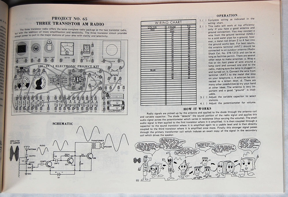
The three schematic views were:
#1. The diagram showing the spring-clip connections required to complete the kit
#2. An Electrical schematic diagram showing the IEEE symbols for the related components.
#3. A "Cartoon" schematic showing how the different circuit elements "helped" each-other to perform the electrical function. In these cartoons transistors danced with LC tank circuits, the speaker was large and loud making sound from electricity.
Ironically it was the "dancing circuits" that I understood last. I don't think the electronics kit was optimally written for a 10 year old learning circuits. I found the #1 and #2 schematics to be most useful given that sometimes there was a mistake in #1. This when I started to memorize schematics in order to help in debug. The above list of schematics reminds me of the "3 Views of circuits".
The three views:
1. Schematic view: Drawn using IEEE or similar symbols
2. Layout view: Drawn using rectangles of different colors (representing different materials)
3. Netlist view: code (text) representing circuits and their related connections.
If you are in analog design you should master all 3 views. This was easier back before Cadence took over the cockpit on Design Automation. In an effort to lower the difficulty of using early CAD software, cadence worked to make everything do-able by a mouse click thereby hiding #3. All views can be used to solve circuit problems, strive to learn them all. More on that in another post..
Back to the schematic:
The Radio Shack schematics were actually pretty good. At the time, I had some magazines from Electronic design magazines such as "Popular Electronics". The old magazine schematics had no real convention and were hard to follow. It turns out that during the "Berkeley Era" analog design renaissance starting in the 1970s schematic methodology improved. Also with good books like Sedra and Smith's Microelectronic circuits we were introduced to a consistent schematic input.
Some key things:
1. Inputs on the left
2. Outputs on the right
3. VDD (Supply) on the top
4. VSS (Ground) on the bottom
5. Clearly labeled currents and node voltages
6. Clearly labeled switches
7. Numerous conventions for ground, signal, earth, vdd, battery
8. Consistent symbols for: Capacitors, resistors, inductors, transformers, tubes, connectors
9. Notes indicating branch currents
10. Notes indicating high voltages
11. Notes to help the layout team understand your design.
12. Good schematic name methodology
13. Logical use of schematic symbols
Far from the "spring clip" days but not too far is the idea that a schematic should convey information. Not a "train-wreck" or "machine generated schematic" but a well drawn schematic can help a person understand, create and even use your circuit.
A good schematic flows with information. Key functions are drawn clearly and near the center of the page. Auxiliary functions are put around the edges of the schematic or at the bottom of the page along with the Revblock. Power-down devices, spare matching devices and the like are placed around the edges often in a box labeled "spare" or "dummies". Input ports are clearly indicated as well as outputs. Avoid drawing in all the NMOS body connections unless you are working on a multi-well process. Drawing clear schematics saves time in that helps the reader understand what the "flow" of the circuit is. Circuits are drawn in such a way as to help the reader. Since we all spend considerable time looking at schematics, its good to spend some time on them. Don't go overboard, since it can be counter-productive. An example is: It is possible to use complicated expressions to connect circuit elements:
node_x<12:4,1,3:2>
I recall (younger) engineers boasting how you can connect up a circuit with a few elements on a page and a list of numbers (as shown above). This is counter-productive for several reasons. For example, during a design review, you will have to explain the connection. You will also have to explain why you chose to hide the connectivity with "cleverness". Your peers will also note that you spent some time figuring out how to make tricky node names when you should have been simply designing a circuit.
Most (but not all) schematics in Analog will be turned into a layout. It is this process of a schematic becoming a layout where most of the trouble in analog comes in. A good designer should be thinking about #1 and #2 above during the design. Yes, you need to visualize the final layout while you are doing the schematic portion of the design. This gets easier with experience. While working on the schematic its important that the layout team be given hints as to what the final form the layout should be in.
Examples of good layout hints:
#1. Identify matching components: M1 matches M2, M3, M4. C1=C2=C3
#2. Identify type of matching: Common centroid, Inter digitized, in the "same row"
a. Also type of environment/area such as "Avoid well edge"
#3. Identify current requirements: Branches identified since 1u copper can only care 1ma of current...
#4. Identify any key pitch required. Some analog layouts are "Row based" and the row geometry should be defined on the schematic
#5. Identify any orientation required. "This resistor match the resistor direction in the Bandgap"
#6. Identify noisy signals that must be shielded against
#7. Identify sensitive signals that must be protected
#8. Identify parts of the circuit that are exposed to light
#9. Identify parts of the circuit that are in the "ESD" network or "Primary or Secondary" ESD structures
10. Identify units for "unit element" type matching arrays
11. Try to avoid components that do not have a layout view since you will be disappointed
12. Bus wires Largest:smallest node<110:0>
13. Bus wires should have thick lines. Single-wires use thin lines
14. Use signal names that are clear and not confusing.
15. Text and drawing layers to help with useful diagrams and notes
Now that we have well annotated clear schematic showing function and giving layout tips, the final task is to give the schematic a good name. Naming conventions on schematics should be such that the schematic's purpose be indicated by its name. Hierarchy is also included in the name. Often the expression "TOP" is used for the top-most level of hierarchy. This is a good starting point. You also would like all the schematics to be "with eachother" and easy to group. Its important that the schematics of a block or subsystem "group" together making them easier to understand. Its counterproductive to keep track of schematics based on peoples names, for example, since they may leave the company or design circuits in several different products. Combining these concepts together I have found that using the circuit name combined with hierarchy work well. With revision control and a title sheet, most all key information can be tracked. In the beginning peoples names may sound like a good way to start but this falls apart after a few products and or process technologies are introduced.
Example of a good set of schematic names:
adc_top
adc_core
adc_analog
adc_digital
adc_refgen
adc_clockgen
adc_stage
adc_stage_comparator
adc_stage_comparator_decoder
If no revision control exists, then you can add further extensions. Often the "rev letter" represents the base-layer generation and "the number" represents the metal connectivity. Normally we prefer to change the metal as this may (sometimes) avoid a "re-qualification" of the product.
adc_top_a1: First metal-rev of ADC_TOP_A0 (a0, a1, a2...)
adc_core_b2: Second metal revision on second set of base-layers (b2)
Never have two schematics of different circuits with the same name. If you want another layout for the same transistor schematic, make a new schematic name with NEW layout comments. Also help the layout designer by letting him or her know that you are leveraging a previous design.
Finally, some schematics are NEVER intended for layout. Those are often "test-bench" schematics or those used for simulation purposes only. I like to name these schematics starting with "zz". I do this since all the test-benches will sit along with eachother in the library when sorted alphabetically.
Finally there are the schematic symbols. If you create your own analog circuits often you will have to provide a "symbol" to allow for the hook-up of your circuit. A good symbol's connection to the rest of a circuit should be obvious. The symbol should have nets clearly indicated and not spaced minimum. The pitch of the symbol should align with the GRID settings used by the team. Its nice to draw a picture on the symbol to help indicate what it does. Often this is a small circuit diagram. Op amp symbols should look like an amplifier. If you have a very large resistor ladder, a schematic can be drawn with a "resistor" on it with tap-points indicated on the symbol. Large resistor and capacitor arrays snaking through schematics can be hard to follow. Sometimes its better if these component arrangements are included within a symbol.
Finally, any special device such as a unit resistor or unit capacitor that is populated in mass on a design should have its own schematic sheet. This is subtle but when a device unit is put on a separate page it forces the layout person also to make an array and not "flatten" the design. This way you can make sure each of your unit elements have the same contact pitch and number, geometry and base-layer connections.
I hope these schematic notes help you and your friends to draw better schematics.
Monday, April 15, 2013
Getting the first job/Memories of Dave Nack
I was on vacation in Mexico when I wrote this about my transition from college to work.
In the final stages of my thesis I set out to interview at several companies and ended up at Level One Communications. Dave Nack was my manager for my first full-time job after graduating college. Dave was an excellent first manager and I am glad I chose the Level One route. Dave and I didn't always agree, but in the end Dave was always correct. The time period was 1998 pre dot-com bust.
My thesis advisors Stephen Lewis and Paul Hurst were involved in the Sacramento electronics scene since they do research in communications and data converters. Paul and Steve are also two of my key mentors (and more about them later). When a company sponsors university research it gets on the thankful students' radars. I am still very thankful and appreciate the companies who helped fund my interleaved ADC calibration work and decided to target those companies first. Level One was one of those companies.
I recall waiting in SSCRL for the Level One phone screen since I didn't have a cell phone and had to use the community lab wireless phone. 5pm went by and no Dave Nack. He didn't call the lab as he was supposed to. So I got on the lab phone and looked up the phone number for Level One on their (new) website. I called the Level one front desk hoping someone was still there. Once I got a hold of phone operator I asked for them to find Dave Nack. I was then transferred to a lab phone number and Dave was in there busy working. He sad "Dave Nack" and I responded "This is (SSA) and how about that phone screen?" Dave responded "We are going to call you back and setup an on-site. The fact you got a hold of me in the lab means you passed the phone screen. Sorry I forgot."
During the interview process I try to treat the companies basically the same, and of course improve as I go along. I used some of my last money to buy a suit at Mens Wearhouse along with a blue blazer. (I prefer to interview in a blue blazer if I can since its a little less formal than the suit.) I would wear that, dress pants and leather shoes. I also wear a tie normally a muted blue or dark red. My father in-law clued me in on an excellent book titled Sweaty Palms: The Neglected Art of Being Interviewed. In this book the author, H. Anthony Medley, discusses interview behavior, styles, how to dress and also how to behave at meals. He also includes a way to reduce the clammy handshake. You can get that book in Kindle for cheap it could 10X your chances of getting a job, based on my interactions interviewing dozens of interns at a previous company. The more prestigious the school, the more they needed Medley's book or so was the trend. I hear that Silicon Valley is "relaxed" but I still don't buy into that as an excuse to show up in blue-jeans and a t-shirt. (As a manager, personaly your odds reduce to near zero if it appears you are not willing to put the effort into getting the job. Is that also how you do design?)
I always come prepared as much as possible for an interview. Get a good nights sleep beforehand. I bring a folder or a small document bag that contains an engineering notepad and a separate notepad with information about the company (my notes from studying the company and its product lines). In addition I would have a calculator (cell phone with calculator), a pen or mechanical pencil, and an extra copy of my resume. Most engineers I know that do interviews still like a whiteboard or paper. If you handwriting is bad stick to paper. Before the interview I try to get the list of people I will meet ahead if possible so I can study their names and titles. There are memory techniques I learned along the way (Kevin Trudeau's Mega Memory) that enable me to memorize the names of everyone I meet. I use the engineering pad during the interview to solve technical problems. If you are fresh out of college this will be a big part of the interview getting and answering technical questions. (Fresh-outs should bring wit, enthusiasm and energy to an interview. Be careful not to over-do it, read Sweaty Palms) I would only take only brief notes during the interview on my non-engineering notepad. That notepad was most useful after the interview. As soon as possible after the interview its good to write notes about everything you experienced, saw, or messed up and compile notes on the people you met. It may take weeks to get through the whole process, you will meet a number of people and may forget a critical detail, so don't be afraid to write 5 or more pages of notes. These post-interview notes will be combined with my initial notes and later used to help size up the opportunity. In the beginning of your career you should be looking for mentors and some stability. A start-up is normally a bad-idea for a fresh-out, since you will probably be abused or be in an unstable situation and NOT have the street-smarts to know it. Running a good IC company is not just technical, it requires a cohesive team. During your interviews if you meet what looks like a good mentor make a note of it. If you find a jerk also make a note of it. Your school network (IEEE, LAB) may also may have some notes and even example questions from their interviewers assuming those students already have taken jobs or eliminated the company you are interested in. I know the SSCRL lab had example questions from hiring managers including Dave Nack. Often students would talk about their interview experiences giving valuable insights.
I interviewed at just under ten different companies. I learned a lot by checking out many companies at the same time. Companies have personalities like people. Their size, age, product lines and where they are located all all factors. Best was small, stable and growing. Worst was "We can pay you low because our company is great and you are new and not worthy." Not realizing I have a choice. Understanding that I was still new to the business I wanted to observe how companies can make decent money on mixed-signal and analog. It came down to two, Crystal and Level One. Level One was the best fit and ironically didnt require I move . The interview at Level One was actually fun and I didn't want to leave. I liked the people, lots of SSCRL grads (Chuc Thanh, Jim Parker, Charles Cai), the noise level (not too quiet), the company was growing rapidly and appeared to be a fun place to work. I met Perry Heedley during that interview yet another reason to work there. There were also many other good technically excellent (and cool) people. Dan Ray was a big influence he liked the mixed-signal DFE work and adapted the concept to a couple of product lines I would later design a transmitter for.
When I make a career decision after interviews I normally turn to a Excel spreadsheet as a tool. I make a scale from 1-10 and pick a weighting where the topmost items on the list have the highest influence. The most important factors I use are personal and yours should be to. The list can generate a custom score for each company you interview with. This is an example of what my list might have looked like:
#1. Will this job make happy/help to accomplish my career goal?
#2. How does the project and company personality fit your strengths?
#3. How would taking the job affect my Spouse (and children)?
#4. How would taking the job affect my extended family? Travel?
#5. How close is this job to friends or people in your network (other places to work)?
#6. How well do I like my potential manager and his reputation?
#7. How-many good potential mentors available? ( - people you didn't like)
#8. How competitive is the salary offer?
#9. How competitive is the whole compensation including benefits.?
#10. Level of opportunity vs. stability
The list is also important if you have to turn down a company since you would have identified what makes it not a good fit. Politely put negative feedback be can be useful to human-resources and potential hiring managers. How were you treated during the interview? Did you wait around? Did you talk to the people who you were supposed to or substitutes? Is the place a mess? In some cases negative feebdack can open up negotiations since most everything is negotiable during an interview process. Some things are easier to negotiate than others. Post college I have added a "life coach" and discussions with key collegues as well as Paul and Stephen.
Level One clearly passed my spreadsheet and gut test, so I took the job after submitting my thesis to the second of the three professor readers required. Its very difficult to write your first thesis draft while working full-time. You are not paid to do your thesis during work hours, so those are done on your own time. Companies will complain about delays but its not uncommon to negotiate a delayed start of a month for a student to get their studies in line. This brings me to another point that employers interview when they are looking for employees. Once they find someone the position (rec) is normally closed. So if you wait till the very end of your studies to interview you may have to pass up a great opportunity. You also have the freedom to reject the not so good jobs Its better to interview and be honest about your readyness than to wait until its all over since starting dates are negotiable. Collect data. Its not a good idea to interview at a company if there is zero chance you will work there. In those cases, you can offer to do a talk at the sponsor's site, saving a lot of time on both sides of the interview table while gaining respect since time=money.
My first job function at Level One was Electrostatic Discharge protection and pads (ESD) since we had a designer going out on maternity leave. Dave was my manager, mentor and was there when I needed him (Along with lots of help from my new friend and mentor at the time, Perry Heedley). Dave would fight for me and go to bat for me. He focused on culture and efficiency, not just getting the most hours of work during a week at minimal cost. (This required long-term, big-picture thinking and planning on Dave's side.) Dave didn't micro manage (Micro-manage=tell you each thing to do often in a list). Micro-management of highly competent people is bad since it stamps out creativity and eliminates feelings of accomplishment and ownership from a job well done thus leading to lower overall product quality. It was amazing and now in hindsight I had no idea how good he was as a manager. Dave worked hard to make sure I got everything I deserved including publication bonuses for university work that overlapped Level One. I try to copy Dave's style when I manage since it creates the positive karma required for a strong and dedicated team. Dave demonstrated that its not all about one person but building a cohesive team (not unlike a basketball team). The LAN group had career advancement potential all within a motivating environment. The transition from college to work wasn't easy for me and I had to work on my personal interaction style and Dave and Perry were very helpful. The biggest challenge I faced was working as part of the team. Its not efficient to do everything yourself so you need to learn the right times and ways to ask for help. On a healthy team everyone wants the chip to work, so its in everybody's best interest to help out new people.
After a few months of ESD I took over the (Gigabit media independent interface) GMII interface for a gigabit ethernet part. Then we had a labor crunch since the AFE was growing in complexity. Gigabit was a huge change for the company being the most complex SOC in the company at that time. Doing the gigabit Ethernet project was almost like trying to swallow too-big a piece of food. The methods of IC design change with the complexity. A brute-force design process can take much longer than expected and also have collateral consequences to other product lines within the company. If not done intelligently this can add huge amounts of cost and delays. (tape-out is a meaningless milestone..) In hindsight, the greatest cost came from a lack of focus on the primary goal of delivering a working reliable product. To combat the ever expanding schedule I ended up taking over the AGC and eventually the ADC debug. Later I would architect the ADC used for future generation 1G products.
To combat the complexity creep in SOCs we would try to stick to a methodology. Schematic signal flow left-right. Avoid drawing in all your bulk ties since they clutter up the schematic. Names should be clear and should not be mistaken for their complemented counterparts. Name power supplies with a number that represents the voltage with an "a" added to specify analog. Short list of passing names:
vdda2p5
vdda1p8
vssa
vddd
enable
reset
adcdataout<7:0>
Now back do Dave Nack, his schematics were quite horrible to look at. He would often use as few pages as possible but they were huge. Where Dave excelled with interface names. Daves signal names were "the best". This is where I came into conflict to Dave for the first time. I got my first review Dave gave me a "needs improvement" on one item, it was my signal naming convention. It wasn't good enough for Dave.
I used an MDAC or "Multiplying Digital to Analog Converter" for the gain-control in the gigabit. (This was based on a constant return-ratio approach from a paper authored by Bret Rothenberg and Paul Hurst.) Part of the MDAC has sampling capacitor array. The more capacitors that sample the input, the higher the gain. So as a key part of the AGC I had bunch of these little "leaf cells" that had a digital control signal on them called "sample". If sample=1, the capacitor in the cell samples the input. By setting more leaf-cell sample signals to 1, the gain of the circuit increases. The center of the block had a centroided grouping of these unit cells. The AGC had a gain range from like 0.5 to 2.5 or something like that, so some capacitor leaf-cells always had sample=1 to give the gain of 0.5. So on those cells I tied sample signal to VDDA2P5. Dave just wouldn't have that.
"Why would anyone connect a sample to a power supply?" Dave asked. I told him its an MDAC and it samples the input when that signal=1. "But its a sampling circuit".. Dave would reply. It dawned on me that Dave didn't fully understand the MDAC. He was confused by the way the "Sample" signal was used, it was interfering with his ability to understand the circuit. It was making him confused. My choice of signal name was a problem.
So Dave did convince me. If there is a signal name that can be interpreted in different ways, or associated with an unrelated function its name should be changed. Normally these bad signal names give them selves away by coming up in group meetings or discussions. I know digital designers don't like to change signal names, but sometimes the work of a few digital designers changing a port listing is less than hours of wasted time in group meetings. Dave is right, if your schematic port-name is unclear or causing complaints, get over yourself and change it.
I miss Dave as he passed away while at work in Irvine some 5 years after we parted ways. As I type this I am sitting on a ship on the mouth of the Sea of Cortez in Mexico thinking about Dave. Dave had a boat and loved to take it on the Sacramento river. He seemed to be most happy when talking about spending time with wife, son and daughter on the river. Its sad that such a great analog talent had to die so young. Sometimes I wonder what life would be like with Dave around. In some ways, I guess he still is.
Subscribe to:
Posts (Atom)